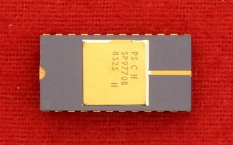
SP9770
Features
- Operating Temperature Range -30°C to +85°C
- 12ns Settling Time 1 LSB Typically
- 10 Bits ± ½ LSB Integral and ± ½ LSB Differential Linearity
- Current Output
- ECL 10K Standard Inputs
- Complementary Outputs, 20mA Full Scale
- Reference Temperature Coefficient Typically 40ppm/°C
Applications
- Data Conversion
- Video Graphic Displays
- Instrumentation
- Waveform Generators
- High-Speed Modems
The SP9770B is an ECL 10k compatible 10-bit DAC. The 12nsec settling time allows a 75 megasample per second conversion time. An inherently low glitch design is used, and the complementary current outputs are suitable for direct transmission line drive. The SP8770B design includes a high-performance voltage reference and reference amplifier.
Output compliance
Pin 17 should be connected to a reference voltage supply at the most positive voltages required with the load, and RSET pin 24 returned similarly to this reference. Conveniently, the reference is ground but this limits the output to negative voltage excursions only. The output compliance can be increased at the expense of linearity.
Operation
The DAC has current outputs, with a nominal full-scale of 20mA, corresponding with a 1-volt drop across a 50Ω load. The actual output current is determined by the on-chip reference voltage and an off-chip current setting resistor. Output current, IOUT is given by:
IOUT = 4 VREF/RSET at full scale
A complementary IOUT is also provided. If single output operation only is employed, it must be ensured that the complementary output is terminated in an identical manner to the used output. The setting resistor RSET is typically 240Ω, giving a full-scale output current of 21mA and should have a temperature coefficient similar to that of the output load resistor. The reference voltage source is -1.280 volts nominal and is of a modified bandgap type. Samples show average temperature coefficients of 50ppm/°C from -55°C to +125°C. This precision voltage reference can be used as an independent part. The reference supply is internally compensated; however, to reduce the possibility of instability or noise generation, pin 21 should be decoupled to ground with a 1nF ceramic chip capacitor. The current loop technique has been used with a high-performance loop amplifier. The current is set by an external resistor as described above. Stabilisation of the loop amplifier is achieved by a single capacitor from pin 23 to ground. Minimum value is 3900pF although a 10nF chip ceramic is recommended.
Multiplying mode
Multiplying operation of the DAC is available in two modes, either a voltage applied in place of the reference or a current supplied via the current source pin. In the former case, the 3dB bandwidth is 250 kHz, while in the latter operational use exceeds 20 MHz.
