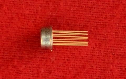
SP8655
Features
- AC Coupled Inputs
- Low Power Consumption
- Open Collector Output CMOS and TTL Compatible
Quick Reference Data
- Supply Voltage: 5.0V
- Power Consumption: 50mW
- Temperature Range: -55°C to +125°C (A Grade)
Description
The SP8655, 57 and 59 are low power emitter coupled logic counters with open collector outputs capable of driving TTL or CMOS. They are available in two temperature ranges: -55°C to +125°C (A grade) and -30°C to +70°C (B grade). They have internally biased inputs.
Operating Notes
- The clock inputs (pin 1 and 8) should be capacitively coupled to the signal source. When driven single-ended, the input signal path is completed by connecting a capacitor from the unused input to ground.
- In the absence of a signal the devices self-oscillate. This can be prevented by connecting a 39k resistor from either input to ground. If the device is driven single ended, it is recommended that the pulldown resistor is connected to the decoupled unused input. There will be loss in sensitivity of approximately 200mV.
- The device will operate down to DC, but the input slew rate must be better than 100V/µS.
- The open collector output will drive 3 TTL loads, and thus a suitable resistor to Vcc is required to maintain noise immunity. For interfacing to CMOS, the open collector may be restored to a +10V line via a 3.3k resistor. The output sink current must not exceed 10mA, and the use of too low a value of resistor may lead to a loss of noise immunity, especially at low temperatures.
- Input impedance is a function of frequency. See figure 4.
- The rise time of the open collector output waveform is directly proportional to the load capacitance and load resistor value. Therefore the load capacitance should be minimised, and the load resistor kept to a minimum compatible with system power requirements. In the test configuration of figure 5, the output rise time is approximately 20ns and fall time is typically 10ns.
