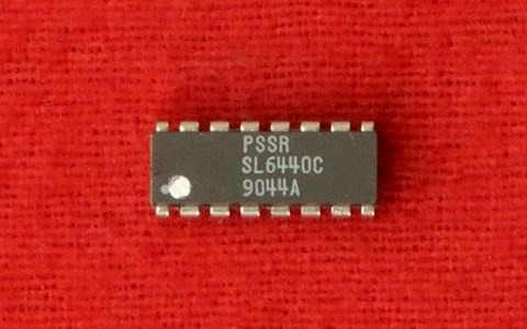
SL6440
Features
- +30dBm Input Intercept Point
- +15dBm Compression Point (1dB)
- Programmable Performance
- -55°C to +125°C Temperature Range
Applications
- Mixers
- Phase Comparators
- Modulators
- SSB Receiver
Brief Description
The SL6440 is a double balanced mixer intended for use in radio systems up to 150MHz. A unique feature of the circuit allows external selection of the DC operating conditions using a resistor connected between pin 11 (bias) and Vcc. When biased for a supply current of 50mA the SL6440 offers a 3rd order intermodulation intercept point of typically +30dBm, a value previously unobtainable with integrated circuits. This makes the device suitable for many applications and offers the advantages of a voltage gain, low local oscillator drive requirement and superior isolation.
The SL6440C (in a 16-lead DIL plastic package) is specified for operation from -30°C to +85°C; the SL6440A (in ceramic case) has a military temperature range specification.
Circuit Description
The SL6440 is a high-level mixer designed to have a linear RF performance. The linearity can be programmed using the IP pin (11). The output pins are open collector outputs so that the conversion gain and output loads can be chosen for the specific application.
Since the outputs are open collectors, they should be returned to a supply VCC1 through a load. The choice of VCC1 is important since it must be ensured that the voltage on pins 3 and 14 is not low enough to saturate the output transistors and so limit the signal swing unnecessarily. If the voltage on pins 3 and 14 is always greater than VCC2, the outputs will not saturate. The output frequency response will reduce as the output transistors near saturation.Minimum VCC1 = (IP x RL) + Vs + VCC2 where
IP = programmed current
RL = DC load resistance
Vs = max signal swing at output
If the signal swing is not known then
minimum VCC1 = 2 (IP x RL) + VCC2
In this case, the signal will be limiting at the input before the output saturates.
The device has a separate supply (VCC2) for the oscillator buffer (pin 4). The current (IP) programmed into pin 11 can be supplied via a resistor from VCC1 or from a current source. The conversion gain is equal to
G=RL*IP/(56.6*IP + 0.0785)
As an example Figure 7 shows typical dissipations assuming VCC1 and V0 are equal. This may not be the case in practice, and the device dissipation has to be calculated for any particular application.
Figure 4 shows the intermodulation performance against IP. The curves are independent of VCC1 and VCC2 but if VCC1 becomes too low the output signal swing cannot be accommodated, and if VCC2 becomes too low the circuit will not provide enough drive to sink the programmed current.
Examples are shown of performance at various supply voltages.
Applications
The SL6440 can be used with differential or single-ended inputs and outputs. A balanced input will give better carrier leak. The high input impedance allows step-up transformers to be used if desired, while high output impedance allows a choice of output impedance and conversion gain.
Figure 2 shows the simplest application circuit. The input and output are single-ended, and Ip is supplied from VCC1 via a resistor. Increasing RL will increase the conversion gain, care being taken to choose a suitable value for VCC1.
Figure 8 shows an application with balanced input, for improved carrier leak, and balanced output for increased conversion gain. A lower VCC1 giving lower device dissipation can be used with this arrangement.
Design Procedure
- Decide on input configuration using local oscillator data. If using a transformer on input, decide on ratio from noise considerations.
- Decide on output configuration and value of conversion gain required.
- Decide on the value of IP and VCC2 using intermodulation and compression point graphs.
- Using values of conversion gain, VCC2, load and Ip already chosen, decide on the value of VCC1.
- Calculate device dissipation and decide whether heatsink is required from maximum operating temperature considerations.
