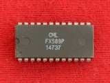
FX589
Features
- Full-Duplex Gaussian Minimum Shift Keying (GMSK)
- Operating from 3 Volts to 5.5 Volts
- Data Rates 4kb/s to 64kb/s
- Selectable BT (0.3 or 0.5)
- Low-Current Analogue/Digital
- Non-DSP Solution
- Meets RCR STD-18
Applications
- Wireless LAN/Modems
- Handy Data Terminals
- Low-Power Wireless Data Link for PCs, Laptops and Printers
- Point-Of-Sale Terminals
- Wireless Bar-Code Readers and Stock Controllers
Brief Description
The FX589 is a single-chip modem employing Gaussian Minimum Shift Keying (GMSK) modulation. Data rates of 4kb/s to 64kb/s and the choice of BT to 0.3 or 0.5 are pin-programmable functions to suit data channel bandwidth requirements.
The Rx and Tx digital data interfaces are bit-serial and synchronised to Rx and Tx data clocks generated by the modem. Separate Rx and Tx power save/Enable inputs allow for full- or half-duplex operation.Rx input levels can be set by a suitable ac and dc level adjusting circuit built, with external components, around an on-chip Rx input amplifier.
Acquisition, lock and hold of Rx data signals are made easier and faster by the use of Rx Control Inputs to clamp, detect and hold input data levels and can be set by the system µProcessor as required.
The indication is available, from the Rx S/N output, as to the quality of the received signal.
The FX589 design features a low-current analogue/digital ASIC process offering significantly lower current consumption than DSP technology. For data rates up to 32kb/s the FX589 draws typically 1.5mA at 3.0 volts VDD and for data rates up to 64kb/s at 5.0 volts, typically 4.0mA.
This low-power CMOS microcircuit is available in both 24-pin plastic DIL and Small Outline (SOIC and SSOP) packages.
Clock Oscillator and Dividers
The Tx and (nominal) Rx data rates are determined by the division of the frequency present at the Xtal pin, which may be generated by the on-chip Xtal oscillator or be derived from an external source.
The division ratio is controlled by the logic level inputs on the ClkDivA/B pins and is shown in the table below - together with an indication of how various ‘standard’ data rates may be derived from common µP Xtal frequencies.
Radio Channel Requirements
To achieve legal adjacent channel performance at high bit-rates, a radio with an accurate carrier frequency and modulation index will be required.
To achieve optimum channel utilisation, (e.g. Low BER and high data-rates) attention must be paid to the phase and frequency response of both the IF and
baseband circuitry.
